

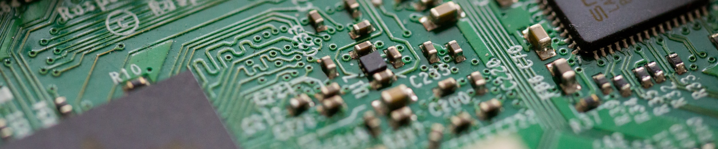
It can be said that Integrated Circuit (IC) design is empowering today’s digital age. From smartphones to sophisticated medical devices, ICs are omnipresent, driving innovation and powering our interconnected world. However, behind every revolutionary piece of technology lies an intricate design process, or called the IC design flow. Let’s delve into figuring out the ic design flow in this below article.
-
What is IC Design Flow?
IC design flow is a systematic methodology encompassing a series of steps to the stage where the IC blueprint is ready to be transferred to semiconductor plant to be manufactured. The output IC product is expected to have desired functionality, performance, and efficiency.
The higher the requirements, the more detailed and complex the IC design flow is. Therefore each IC type on the market aligns with multiple IC design flows. Yet, no semiconductor design engineers can complete an IC “blueprint” without following this basic IC design flow.
-
Key Steps in IC Design Flow
– Specification and Architectural Design
The journey begins with comprehensive specification and architectural planning. In collaboration with stakeholders, engineers define the functionality, performance targets, power constraints, and other critical parameters of the IC. This phase lays the groundwork for subsequent design stages, establishing a clear vision and roadmap for development and suitable technology selection.
In this stage, design engineers should be able to answer these questions:
- What is the IC made for?
- What functions must the IC deliver?
- What is the required speed and power consumption?
- What is the target cost?
– Design Entry – Logic/Circuit Design
Once objectives/ specifications are in place, designers embark on the design entry phase of the IC design flow, where they conceptualize the circuitry and logic necessary to perform the desired functionality. This involves selecting appropriate circuit components (IC pre-existing blocks), defining interconnections, and crafting the overall macro-level architecture of the IC using a specialized design software tool called logic synthesis. If the macro-level building blocks need to be adjusted to meet the high requirements of the IC, custom circuit design approaches will be applied.
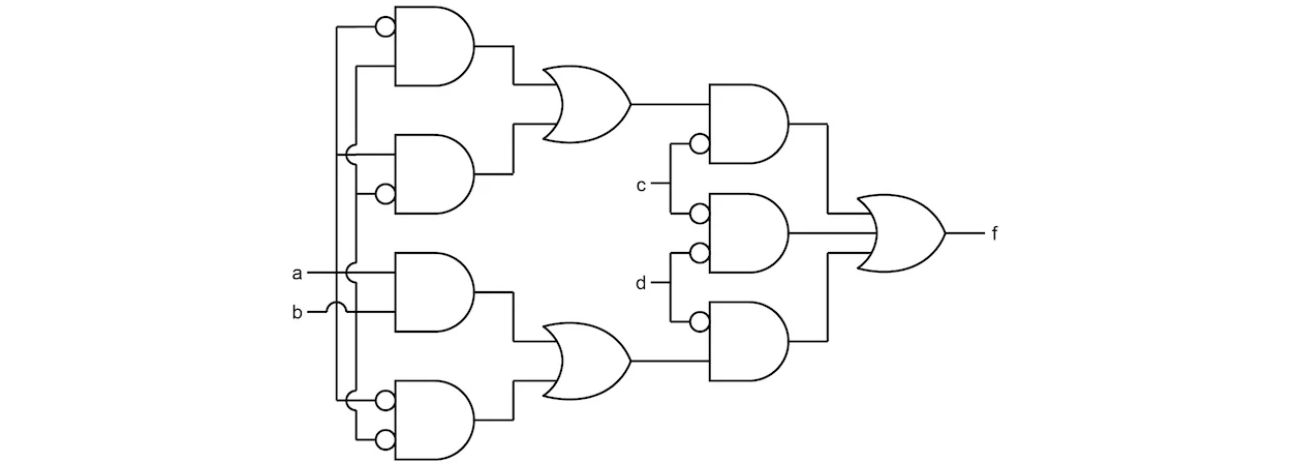
Example of Logic Design (Source: All about Circuit)
Logic synthesis is a pivotal stage wherein the high-level design description is translated into a register transfer level (RTL) representation. Design abstraction techniques are employed to optimize the circuit’s logic structure, minimize power consumption, and enhance performance. Short sum up, this stage defines how the IC will be implemented.
– Physical Design
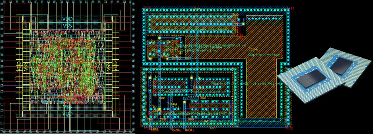
Example of Physical Design
The physical design phase focuses on translating the logical representation of the circuit into a physical layout tailored for fabrication. This involves floor planning, placement, routing, and optimization of the IC layout to meet stringent design constraints such as area, power, and timing requirements, ensuring the desired functionality Cutting-edge tools and methodologies are employed to ensure optimal utilization of silicon real estate and achieve high manufacturability as it assists in analyzing the chip area, delay, congestion, etc.,
– Physical Verification
Moving to the next stage of the IC design flow is the verification stage, an iterative process crucial for ensuring the correctness and robustness of the design. Various techniques, including simulation, formal verification, and emulation, are employed to model the physical effects of the IC (resistance, crosstalk, etc.), detect defective design, ensuring compliance with the specified requirements. Additionally, testing methodologies are employed to validate the IC’s functionality under diverse operating conditions and test cases (wiring, signal crosstalk, etc.). Calibre, Tessent, mPowerm,… are among the software systems assisting the physical verification.
In other words this stage helps designers to visualize how the circuit will be laid on the silicon wafer and measure how it can function under stress.
– Signoff (DFM – DFT and fabrication)
This is the final step in the IC design flow before the design is sent to the manufacturing fab. All of the critical parameters that will impact the performance or manufacturability of the chip are verified against the results of “golden signoff” quality tools, including DFM and DFT.
- Design for Manufacturing (DFM) strategies are integrated into the design flow to enhance manufacturability and maximize yield.
- Techniques such as Design for Testability (DFT), lithography-aware design, and layout optimizations are employed to mitigate manufacturing variations, improve yield, and minimize post-fabrication defects.
In this stage, the design, as well as manufacturability rules are fully verified. As the verification is completed, the final design data is transferred to the semiconductor foundry for fabrication. The design files, along with foundry-specific guidelines and requirements will be sent to the semiconductor plant. Once the design is taped out, the semiconductor manufacturing process begins, involving wafer processing, photolithography, etching, and packaging to transform silicon wafers into functional ICs.
-
Common Types of IC Design
Although the above key steps in the IC Design Flow is the basis for designing any semiconductor chip, depending on IC types, the IC design flow will be distinct. Let’s have a look into the IC design flow of the 4 most common types of IC design:
- Digital IC • Analog IC • RF IC • Mixed-signal IC
-
Digital IC Design Flow
Digital IC design flow involves turning specifications and features into digital blocks, which are then converted into logic circuits. Many of the constraints in digital IC design originate from the foundry process and technological limitations.
| Design Specification
(Specifications → Constraints → Test benchmark development) |
| High-level system design
(Design Partition → Entry-Verilog Behavior Modeling → Functional Verification → Integration & Verification) |
| Logic Synthesis
(Convert Register Transfer Level (RTL) into netlist → Design partitioning in physical blocks → Identify timing margin and constraints → RTL/ gate level netlist verification → Timing analysis) |
| Floorplanning
(Place IC blocks in hierarchical order → Power and clock planning) |
| Synthesis
(Timing constraints and optimization → Static timing analysis → Update placement → Update power and clock planning) |
| Block Level Layout
(Complete blocks placement and routing) |
| IC Level Layout
(IC integration of all blocks → Place cell → Scan chain/clock tree insertion → Rout cell → Physical and electrical design rules check/ verification (DRC) → Layout versus schematic (LVS) → Extract parasitic → Verify post-layout timing → Create GDSII → Tape-out) |
-
Analog IC Design Flow
Analog Integrated Circuit – IC design flow involves creating electronic circuits that manipulate continuous signals, such as voltages and currents, as opposed to digital signals. These circuits are designed to perform more personalized functions like amplification, filtering, modulation, and signal processing, in comparison with Digital ICs.
| Design Specification
(Specifications → Constraints → Topologies → Test benchmark development) |
| Schematic flow defining
(System-level schematic entry → Stimulate architecture HDL → Block HDL specification → Circuit-level schematic entry → Stimulate and Optimize Circuit) |
| Physical flow
(PCell-based layout entry → Design rule check/ verification (DRC) → Layout versus schematic (LVS) → Parasitic extraction → Post-layout simulation → Tape-out) |
-
RF IC Design Flow
RF IC (Radio Frequency Integrated Circuit) design is a specialized field within integrated circuit (IC) design that focuses on creating electronic circuits specialized tailored to operate at radio frequencies. These circuits are used in various wireless communication systems, such as mobile phones, Wi-Fi, Bluetooth, radar systems, and satellite communication. This includes components such as amplifiers, mixers, oscillators, filters, and modulators/demodulators, among others.
Considered as a niche branch of the analog IC, RF IC performs more personalized functions to be used in end products. Therefore, RF IC design flow is often an iterative process that involves the extensive use of EM simulation, parasitic modeling, and package modeling.
| Design Specification
(Specifications → Constraints → Topologies → Test benchmark development) |
| System design
(Design high-level system design and plan budget → Behavioral modeling) |
| Circuit Synthesis
(HDL Mixed-level SIM → Mixed-level partitioning) |
| Circuit Design
(Implement foundry design kit → Spiral inductor synthesis/modeling → Design circuit in detail) |
| Circuit Simulation
(Time and frequency domains) |
| Physical Design
(Layout → Stimulate and extract electromagnet → Parasitic extraction → Extract on-chip passives → Extract package parasitics → Design rules check/verification (DRC) → Layout versus schematic (LVS) |
| System Verification (follow test benches) |
| Signoff |
-
Mixed-signal IC Design Flow
A mixed-signal integrated circuit (IC) is a type of integrated circuit that combines both analog and digital circuitry on the same chip. It integrates analog functions, which deal with continuous signals, and digital functions, which process discrete signals represented as binary numbers. Mixed-signal ICs are widely used in various applications, including data converters (such as analog-to-digital converters and digital-to-analog converters), sensor interfaces, power management, communication systems, and audio processing, etc.
The term “mixed-signal” reflects the combination of analog and digital components within the same IC:
- Analog components handle continuous signals, which can represent physical quantities such as voltage, current, temperature, or pressure.
- Digital components process discrete signals represented as binary values (0s and 1s).
As new IoT, wireless communication (e.g., Wi-Fi, 5G cellular, LoRa, etc.), and sensing technologies are leading the modern society mixed-signal ICs are becoming more and more complex, advancing to meet high-level of requirements.
| Domain Design Specification
(Analog/RF: Schematic capture → Analog simulation Digital: Design entry → Behavioral simulation) |
| Mixed-signal analysis |
| Physical design
(Analog/RF: Physical layout → Physical verification → Post layout simulation Digital: Synthesis → Place and route → Functional verification) |
| Chip assembly & physical verification |
| Mixed-signal functional verification |
| Signoff |
In conclusion, understanding the Integrated Circuit (IC) design flow is fundamental in crafting microchips that shape our modern world. From the inception of specifications to the meticulous physical verification processes, each step in the IC design flow is crucial in ensuring the functionality, performance, and efficiency of ICs. Whether it’s digital, analog, RF, or mixed-signal IC design, the systematic methodologies of IC design flow act as the core basis of making effective, manufacturable chip blueprints.
>> Read more Semiconductor Blogs HERE