

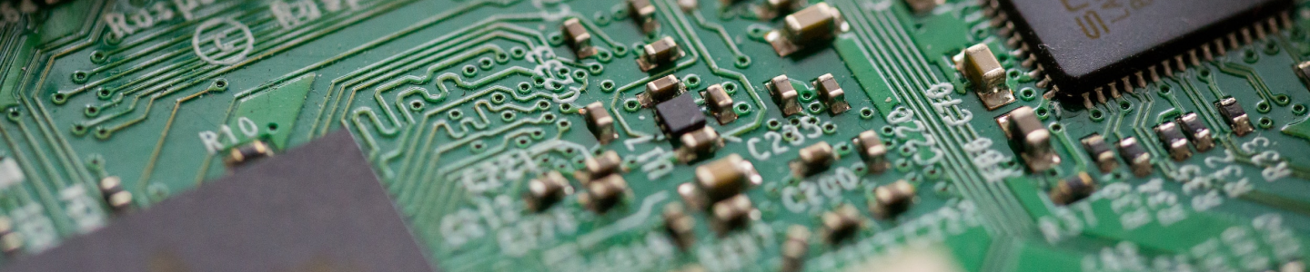
A wafer, or silicon semiconductor wafer, is a crucial physical component in the semiconductor chip production process. It serves as a container for “depicting” the elements that constitute the final chips. Wafer manufacturing, also known as wafer processing, is the very first step in the semiconductor chip production process. In this article, let’s figure out the process of silicon wafers production, in terms of their components, structure, and operating mechanisms.
1. Why is Silicon Commonly Used in Electronics?
Materials in solid states are typically categorized into three types: insulators, semiconductors, and conductors. Among them, insulators (usually ceramics) resist the flow of electric current, while conductors (usually metals) efficiently conduct electricity. Semiconductors, on the other hand, found in between, possess the ability to conduct electricity at a level between insulators and conductors. This property allows semiconductors to control the flow of current between various components within electronic devices, making them a key element in the production of integrated circuits (semiconductor chips).
Up till now, the most common semiconductor material is Silicon, widely applied in the microchip manufacturing industry. While Silicon may not be the most efficient semiconductor, it is the most suitable element for mass production and integration of thousands or millions of electronic components.
What is more, as one of the most abundant elements on Earth, Silicon is the second most prevalent in the Earth’s crust (constituting 27.7%), following Oxygen (46.6%). This has made Silicon an exceptionally attractive material for chip manufacturers in general, and Silicon wafers in particular.
2. How is a Silicon Wafer Produced? (8 steps in wafer manufacturing)
2.1 Pure Silicon Extraction
As mentioned earlier, Silicon exists in the Earth’s crust, yet, it isn’t available at instant. It is extracted from sand (primarily composed of Silic). In its natural state, Silic has too much oxygen to become Silicon. Therefore, it is mixed with Carbon and melted at temperatures exceeding 2000 degrees Celsius to separate Silicon from impurities like Calcium or Aluminum, leaving a product that is 99% pure.
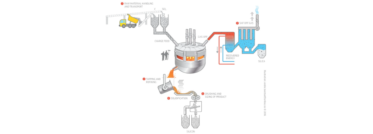
Figure 1. Diagram of the Pure Silicon Extraction Process
However, to optimize semiconductor performance, Silicon must be as pure as possible, ideally close to 100%. Extracted Silicon is then ground into a fine powder (< 40 μM) and then fed into a Fluidized Bed Reactor (FBR), where it reacts with Hydrochloric Acid (HCL) at a temperature of 575K (about 300 degrees Celsius) and is heated until it turns into a liquid.
Then after a series of distillation and evaporation processes, the final product is a Silicon with a purity of 99.9999%.
2.2 Some Polysilicon Growth Method
- Czochralski Method (Cz)
Following the purification process, the next step in Silicon wafer production is creating a Silicon cylinder (Silicon Ingot). The Czochralski method is carried out in a vacuum chamber called a “crystal puller” containing a large metal crucible, typically made of quartz, and an electrically heated component. Vacuuming removes air from the chamber to prevent silicon oxidation. The electrically charged crucible is heated to a temperature sufficient to melt Silicon (above 1421 Celsius).
Once the Silicon charge is completely molten, a small crystal seed, attached to a rod, is lowered into the molten Silicon. This crystal seed, typically around 5 mm in diameter and up to 300 mm in length, acts as a “seed” for the growth of a larger silicon crystal after melting.

Figure 2 . Czochralski Process Flow Diagram (b) Processing Equipment
The “seed” crystal is attached to the rod (ingot) with a known crystal face, oriented vertically during the melting process. The crystal’s growth from the melt will align with this initial orientation, giving the final single crystal a crystallographic orientation similar to the “seed” crystal. After soaking in the melt, the crystal seed is slowly pulled out of the melt at a controlled rate (a few cm per hour) as the larger crystal develops. The pulling speed determines the final diameter (size) of the large crystal. during the crystal-pulling process, both the crystal and the melting crucible are rotated to improve the uniformity of crystal distribution and impurities. The final large crystal has a cylindrical shape, completing the process of creating a single-crystal Silicon.
The Czochralski method is the most cost-effective way to produce large single crystal Silicon blocks. This method can create blocks (ingots) large enough to produce wafers with diameters up to 450 mm. However, the method has certain limitations. As the Silicon crystal blocks are created in quartz crucibles (SiO2), Silicon gets contaminated with Oxygen (existing at 1018 atoms cm-3 or 20 ppm). To address this, manufacturers replace quartz crucibles with crucibles made of graphite, but this creates Carbon impurities in Silicon, although at low concentrations.
Both oxygen and carbon impurities contribute to the reduction of the diffusion length of charge carriers in silicon semiconductor wafers, posing challenges in achieving semiconductors with resistivity greater than 100 ohm-cm.
- Float Zone (Fz) Method
In modern Silicon wafer production, an alternative method to create high-purity single-crystal Silicon is the float zone (Fz) refining method.
In this method, a polycrystalline Silicon rod (ingot) is vertically mounted in a growth chamber, either in a vacuum or inert gas atmosphere. The rod does not come into contact with any components of the chamber except for the surrounding atmosphere and the seed crystal (orientation known) at its bottom(Figure 4). The rod (ingot) is heated using non-contact radio-frequency (RF) inductive heating to create a molten material zone within the rod (typically about 2 cm thick). In the FZ process, the rod moves vertically downward, allowing the molten zone to move upwards along the length of the rod, pushing impurities in front of the molten zone and leaving the result – high-purity single-crystal Silicon.
Fz Silicon wafers have high resistivity of up to 10,000 ohm-cm.

Figure 3 . Float Zone Crystal Growth Configuration.
Once Silicon blocks are created, they are cut into manageable-length pieces, completing the process of creating a single-crystal Silicon ingot.
2.3 Single-Crystal Silicon Ingots (Boule) Orientation
Once the silicon boule has been created, it is cut into manageable lengths and each length is ground to the desired diameter, ranging from 100mm to 450mm (approximately 4 inches to 18 inches). Orientation to represent the type of silicon dopant is also done at this stage. For wafers with a diameter below 200mm (< 8 inches), the largest orientation flat, also known as the primary flat is added perpendicular to a specified crystal axis such as <111> or <100>. The secondary orientation flat (the smaller one) represents the type of dopant (whether it is n-type or p-type) of different wafers.
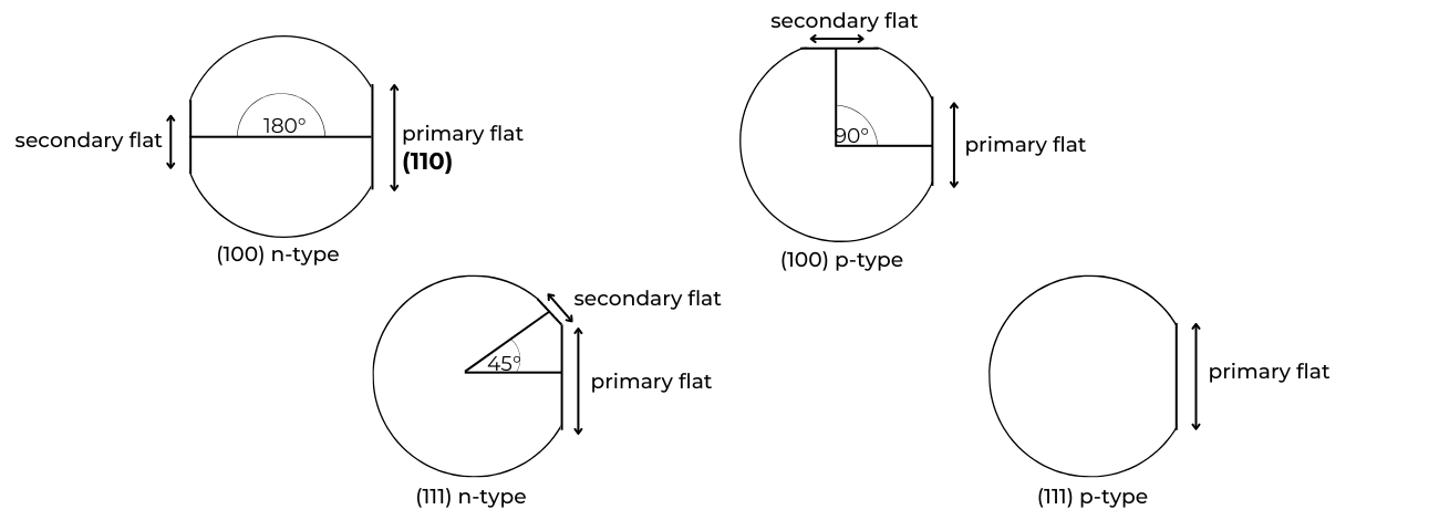
Figure 4: Semiconductor Wafer Flat Symbols for Orientation and Dopant Phases
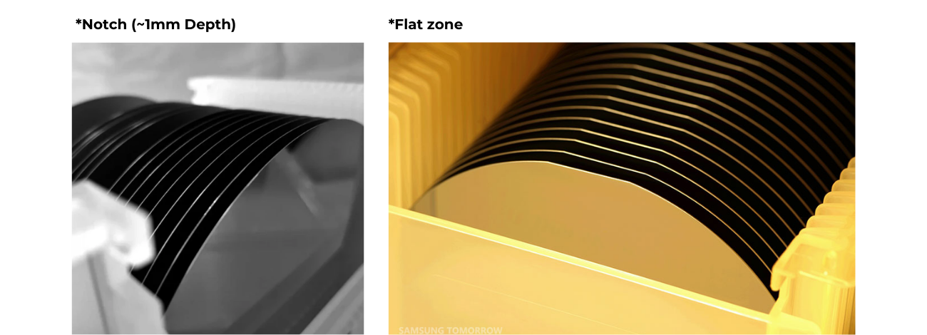
Figure 5
For wafers with a diameter above 200mm (> 8 inches), it uses a single groove along the crystal axis to represent the orientation of the silicon wafer without the indicator for doping type.
2.4 Wafer Slicing
Silicon wafers are cut using a circular blade with embedded diamond splinters. After slicing, the wafer surfaces are relatively flat and smooth, therefore, reducing the time and effort required for subsequent grinding. However, only a single wafer on each diamond saw can be cut at a time, making this technique less productive than grinding (cut by wire saw).

Figure 6: Wafer Slicing With Inside Hole Saw (Annular Saw)
To enhance productivity, a multiple-wire approach is used, allowing the simultaneous cutting of multiple wafers at a time. A high-quality steel wire, up to 100 km in length, with a diameter ranging from 100 to 200 μm, is wound around a rotating roller featuring hundreds of evenly spaced grooves. The wire saw operates at a speed typically about 10 m/s and is coated with diamond particles or wetted with a slurry of abrasive particles like diamond or silicon carbide, along with a carrier fluid (glycol or oil).
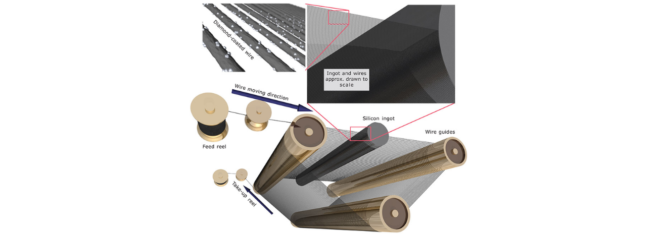
Figure 7: Diagram of wafer slicing technique, using a diamond wire
The primary advantage of this wire saw method is its ability to cut hundreds of wafers simultaneously with a single wire. However, the sliced wafer surface is more bumpy and more uneven compared to wafers cut with a circular saw. Thus, those wafers require a longer time for subsequent grinding processes.
2.5 Chamfering, Grinding (Lapping)
The single-crystal silicon rod (ingot) is sliced into wafers, whose sharp edges need to be cut into circular arcs. This is primarily done to prevent the edges of the wafer from cracking and to address any imperfections in the crystal lattice.

Figure 8: Chamfering the edges of the wafer into circular arcs.
After the cutting phase, there are inevitably some grooves on the surface of the silicon wafer. It is crucial to eliminate these saw marks and surface damage caused by the cutting process through grinding. This step aims to enhance the flatness, curvature, and parallelism of the single-crystal silicon, ensuring it meets the technical requirements of the polishing process later.
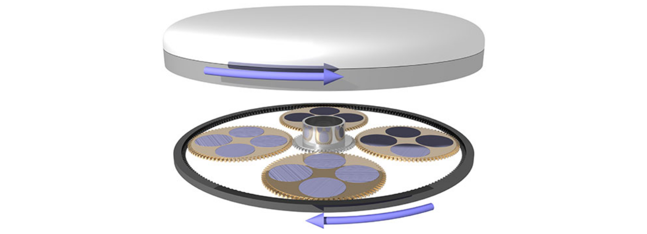
Figure 9: Grinding to remove surface damage caused by cutting.
2.6 Surface Etching & Polishing
The process of cutting and grinding silicon wafer diminishes the crystal structure of the silicon wafer surface. Subsequently, these wafers undergo etching using KOH-based or HNO3/HF-based chemical etchants to eliminate damaged surface areas.
Following this, is a wet chemical-mechanical polishing (CMP) process, with a view to achieve a high-reflectivity surface without scratches and damage on one side of the semiconductor wafer. The chemical etching process involves using a solution of hydrofluoric acid (HF) mixed with nitric acid and acetic acid to dissolve silicon. In CMP, silicon wafers are mounted on a holder and placed in a CMP machine, where they undergo a combined chemical and mechanical polishing process. Typically, CMP uses a hard polyurethane polishing pad along with a mixture of fine abrasive particles such as alumina or silica dispersed in an alkaline solution.
The final product of the CMP process is a silicon wafer with a highly reflective, “mirror-like” surface, with no scratches and damage on one side, suitable for the fabrication of semiconductor chips.
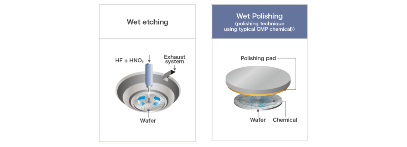
Figure 10: Chemical-Mechanical Polishing (CMP) – Wet Polishing.
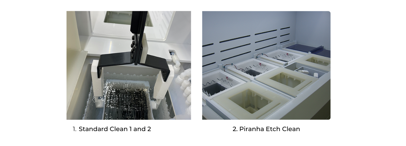
2.7 Cleaning
In the production of modern devices, the wafer-cleaning process can constitute 30% – 40% of the total manufacturing process, underscoring the significance of cleaning semiconductor wafers and treating the underlying surface.
Before entering the wafer manufacturing process, the wafer’s surface must undergo cleaning to eliminate any adhering particles and organic/inorganic contaminants. Silicon oxide must also be removed. Contaminants on the wafer surface can exist in the form of ions and adsorbed elements, thin films, loose particles, particle clusters, and absorbed gases.
The chemicals used in the standard semiconductor wafer cleaning process have remained unchanged for the past 40 years. It relies on employing the RCA cleaning procedure using a solution of hydrogen peroxide and ammonium hydroxide with acidic properties. While this method continues to be the primary approach in the industry, recent developments involve integrating this method with newly optimized cleaning technologies, including ozone and ultrasonic cleaning systems, as highlighted by Modutek.
According to Modutek, the wafer-cleaning process includes the following steps:
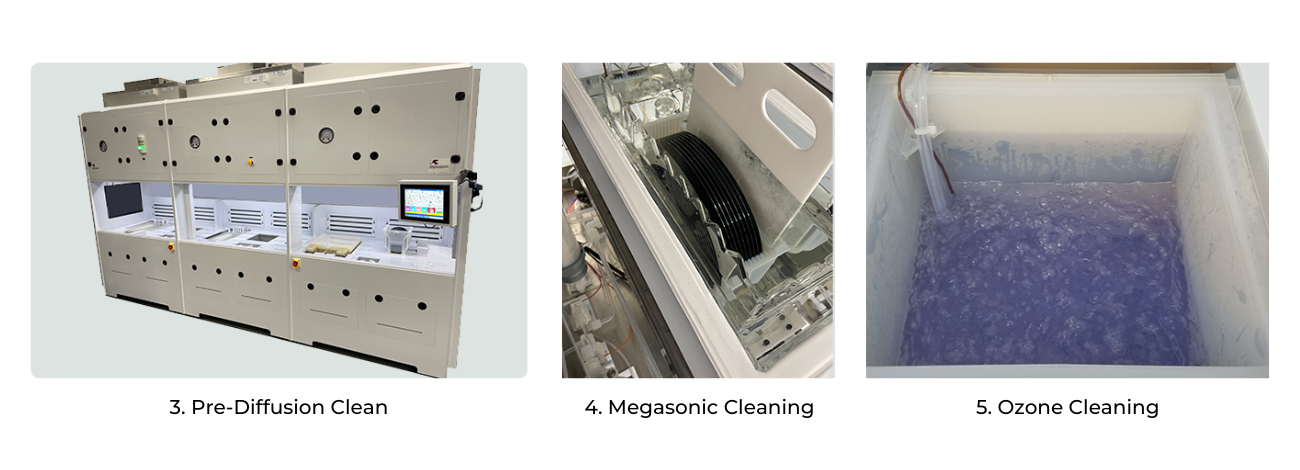
Source: Modutek
2.8 Testing
Now that a complete wafer is in hand, it is crucial to ensure its optimal functionality and suitability for operational demands. The two major threats to silicon wafer integrity are electricity and solvents, as these are the primary causes leading to damage or fractures. To mitigate these risks, manufacturers subject semiconductor wafers to various tests using computer-controlled probes. These probes meticulously examine each section of the wafer; if the criteria are met, the wafer is deemed ready for distribution. In case of failure, the silicon wafer is marked and sorted out of the batch.
After the economic downturn, as well as the peak of the chip crisis in the 2022-2023 period, the global semiconductor industry is poised to recover and resume growth starting in 2024, with growth projections reaching up to two digits. This resurgence forecasts significant potential for growth in the silicon wafer semiconductor manufacturing sector, given its pivotal role in semiconductor chip production, second only to the design phase.