

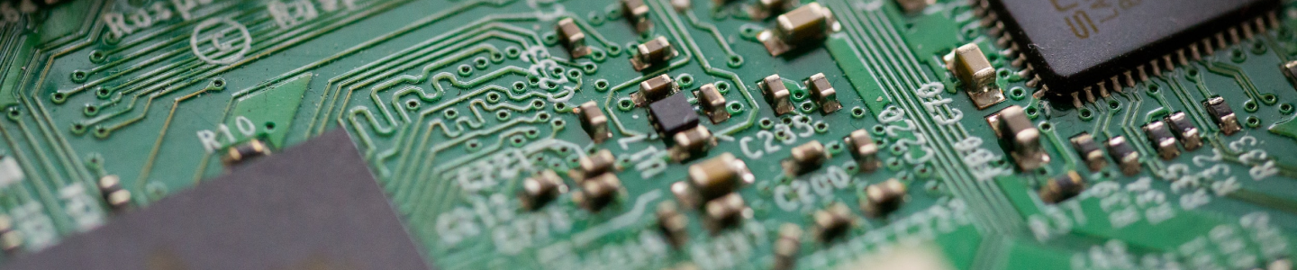
Semiconductor chips play a pivotal role in powering the digital revolution, enabling the devices we rely on daily, from smartphones to computers and beyond. The process of manufacturing these tiny, yet powerful chips involves a series of intricate steps, each contributing to the creation of a functional and efficient semiconductor device. In this blog, we’ll embark on a comprehensive journey through the semiconductor chip manufacturing process, exploring stages from wafer production to the final packaging.
Wafer Manufacturing
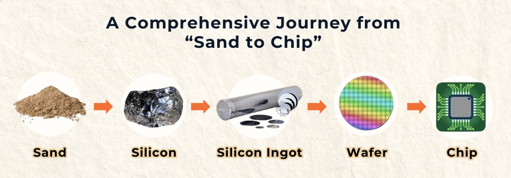
The semiconductor chip manufacturing process begins with the creation of silicon wafers, which are made of sand. These wafers are typically considered the foundation for any semiconductor chip. Producing silicon wafers from tiny grains of sand (also known as Silicon dioxide (SO2) requires quite a sophisticated process:
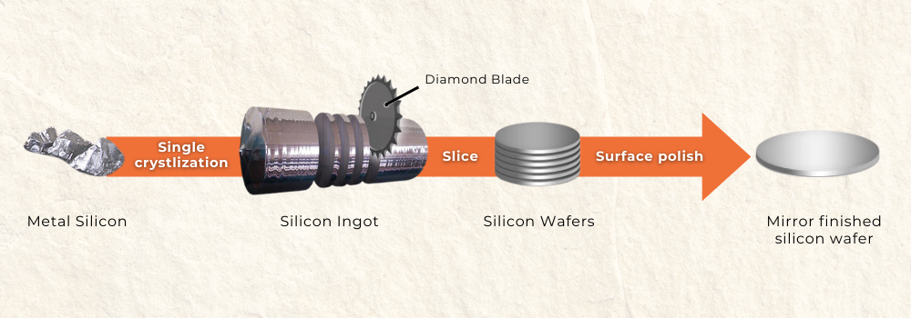
1- First, sand is heated until it melts into a high-purity liquid and then gets solidified by crystallization.
2- After getting the resultant of high-purified silicon pillars, also called ingot cylindricals, these ingots are then sliced into ultra-thin, precise size wafers using advanced diamond saws. With the technology development, typical wafer thicknesses now range from 675 to 725 micrometers.
3- Wafer slices then remain rough and contain defects after cut can affect the electronic IC performance, in terms of precision and function. Therefore, wafers undergo precision polishing to achieve a flawless, mirror-like surface.
Why call them “wafer”? The pattern grinds on the surface with the appearance of a wafer-like is the most simple, yet obvious answer. Depending on the size of the wafer, the number of chips produced is indicated. In simple words, larger equals better capability.
Oxidation
The results wafers are not yet semiconductive to be used. To enhance the electrical properties of the silicon wafer, a thin layer of silicon dioxide (SiO2) is formed on its surface through oxidation. This oxidation stage in the semiconductor chip manufacturing process involves
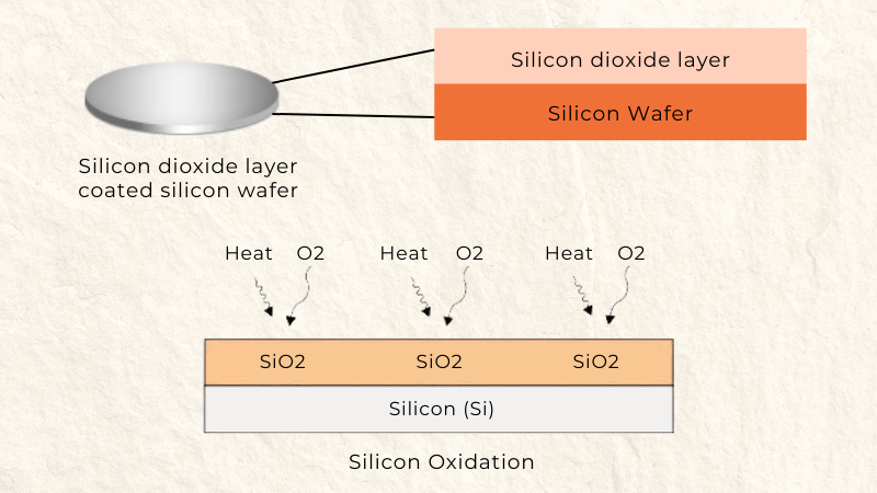
1- Exposing the wafer to high temperatures in the presence of oxygen or water vapor (also known as dry and wet oxidation – the most two common types of oxidation to create a thin, dense layer of silicon dioxide (SiO2) on the wafer’s surface
2- The thickness oxide layer directly affects the performance of the chip therefore, it need to be highly controlled. Modern oxide thickness can now remain at a few nanometers.
3- The silicon dioxide layer serves as an insulator a protective shield, preventing unwanted electrical leakage between different chips on the wafer.
Photolithography
Photolithography is a key step in defining the intricate patterns that form the chip’s circuitry. In other words, it likes “printing” the circuit design onto the wafer, using a technique similar to creating a film camera photo.
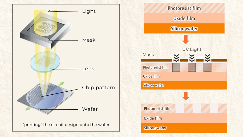
The photography process:
1- First, a thin layer of light-sensitive photoresist is applied to the wafer
2- Then, a photomask – a glass substrate containing the desired circuit pattern design is prepared to selectively expose the photoresist.
3- Let light transfer through the photomask, imprinting the chip design on the wafer surface
Make sure to conduct an additional check to ensure the circuits are drawn well. This step defines the locations for later stages of the semiconductor manufacturing process like etching and deposition.
Etching
The next step in the semiconductor manufacturing process is called etching.
As the chip design is printed on the wafer surface in the photolithography process, it is now time to remove unnecessary material from the wafer’s surface according to the desirable patterns defined by photolithography.
There are two common methods of etching: wet etching and dry etching
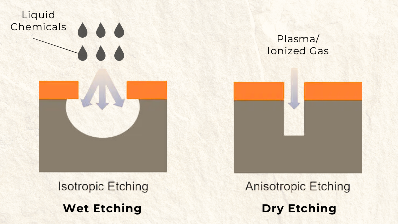
| Wet etching | – A chemical solution, using liquid reactive chemicals to dissolve unwanted materials |
| Dry etching | – Solution using plasma, using ionized gases to selectively remove unwanted material |
It can be said that this step shapes the various components of the chip, including transistors and interconnects, set the fundamental for the miniaturization of electronic IC, which indicates the performance, efficiency and cost.
Deposition
In a chip manufacturing, photolithography and etching process are repeated serveral times, thin layers by thin layers on the wafer. To build the chip’s components, thin layers of materials such as metals and insulators are deposited onto the wafer’s surface.
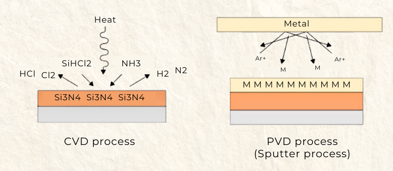
Chemical Vapor Deposition (CVD) and Physical Vapor Deposition (PVD) are common techniques. These coating layers contribute to the formation of transistors and interconnects, with each layer carefully designed to meet specific performance requirements.
Ion Implantation
Semiconductor made of silicon doesn’t conduct electrical characteristics. Therefore, this is the time for ion to be implemented, by adding impurities, altering the ability to conduct electrical properties.
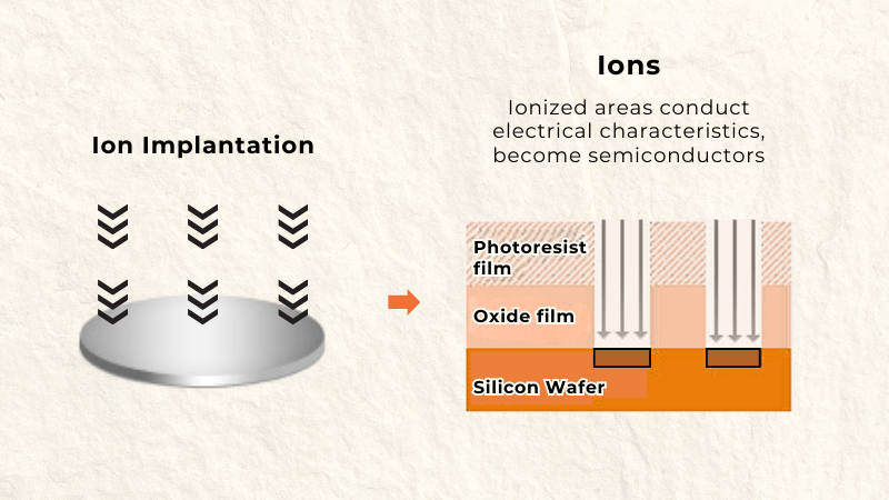
This precise doping process is essential for creating the necessary conductivity variations, cn be considered as the ending phase to make the wafer conductive with a number of chip drawn on it.
Metal Wiring
The addition of metal wires is crucial for establishing electrical connections, creating pathways between various components of the chip. These metal layers, typically made of materials like aluminum, titanium, or stungsten serve as the conductive pathways for electrical signals to flow in the circuit, ensuring efficient communication within the semiconductor device.
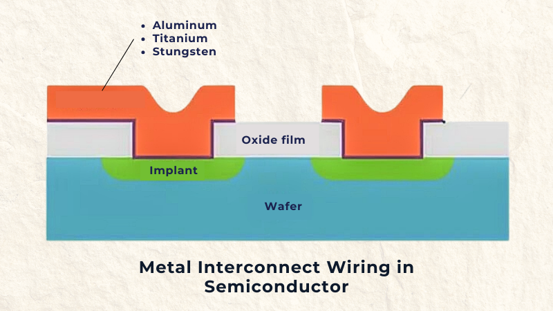
Note: Among those above materials, Aluminum is the most used option as it adheres well to the oxide layer (silicon dioxide) and is easily workable.
Sorting
Once the manufacturing steps are completed, wafers undergo rigorous testing to identify and sorting out defective chips. This stage is also called EDS, or Energy Dispersive Spectroscopy.
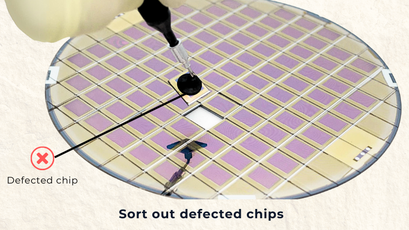
Automated testing equipment assesses each chip’s functionality, ensuring that only fully operational units progress to subsequent stages. This step is critical for maintaining high yields and quality in semiconductor production.
Packaging
Coming to the last phase in the semiconductor chip manufacturing process, the wafer is diced into individual chips. Those chips are then encapsulated in protective casings, connecting it to external pins or leads, enabling electrical exchange with the outside, and ensuring effective heat dissipation. Packaging not only protects the chip from various environmental factors but also influences its overall performance and reliability.

After final test, sealing and labeling of the product name, manufacturer name, the semiconductor chip we commonly see is completed.
Conclusion
The semiconductor chip manufacturing process is “a symphony” of cutting-edge technologies, precision engineering, and scientific ingenuity. From the creation of silicon wafers to the intricate steps of oxidation, photolithography, etching, deposition, ion implantation, metal wiring, sorting, and packaging, each phase contributes to the production of high-performance chips that empower our modern world. As technology advances, the semiconductor industry continues to push the boundaries of what is possible in electronics and computing, driving innovation and shaping the future of interconnected, electrical devices.